Tuesday, March 22, 2011

NiMH Battery Charger


Here is a simple battery charger for the Nickel Metal Hydride battery that requires current regulated charging. The charger provides 140 mA current for quick charging of the battery.Power supply section consists of a 0-18 volt AC 1 Ampere step-down transformer, a full wave bridge rectifier comprising D1 through D4 and the smoothing capacitor C1. Current regulation is achieved by the action of R1,R2 and the Epitaxial Darlington PNP transistor TIP 127. Resistor R1 keeps the charging current to 140 milli amperes. LED and resistor R2 plays an important role to control the base current of T1 and thus its output.


Around 2.6 volts drop develops across the LED which appears at the base of T1. Emitter – base junction of T1 drops around 1.2 volts. So 2.6 – 1.2 volts gives 1.40 volts. So the current passing through R1 will be 1.40 V / 10 = 0.14 Amps or 140 Milli Amps. The LED act as the charging status indicator. LED lights only if the battery is connected to the output of circuit and the input voltage is normal.

Read more: http://electroschematics.com/6073/nimh-battery-charger/#ixzz1HL7dzmz5

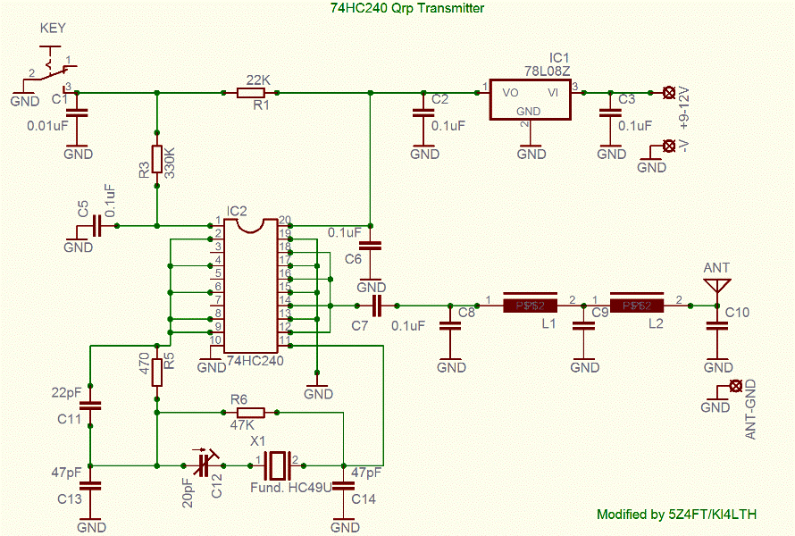
74HC240 Qrp Transmitter.


Description.

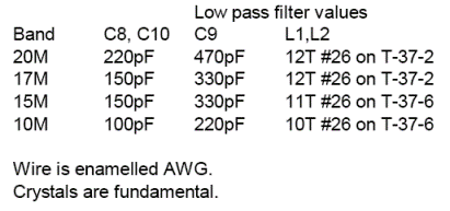
The ARRL HB describes an experimental 0.5W transmitter that uses a 74HC240 octal inverting buffer. One section is used as a fundamental frequency oscillator, four sections are used as an amplifier, while three sections are grounded, and unused. The three unused sections can be put to use in further expansion into a TCVR. Q1 is used to key the transmitter, while the 7808 provides a stable 8V DC supply. THe IC will dissipate heat, and a heat sink should be glued onto it using epoxy. The low pass filter is standard, and the values for some HF bands are given in the table above. This design forms the basis of a minimal QRP TCVR that I am developing, as part of my education in electronics.

http://www.qsl.net/5z4ft/74hc240qrp.html

Saturday, March 19, 2011

Broadband Linear Power amplifier

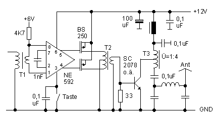
A broadband output transformer in lieu of the parallel tuned circuit is also worth a try. The 10-ohm emitter resistor, capacitor C1 and the 10 uH choke all disappear if FETS are employed. This design probably represents an all-time low in parts count to achieve 1 watt of linear power output, with only 8 components. Note, however, that the 2N3906's actually produce 50% more output for very little added complexity. We could stop at this point, connecting our 1-watt powerhouse to an antenna (via a low pass filter, of course!), or use this circuit to drive an a RF power transistor of more substantial proportions, as shown below. Depending on the frequency, we can achieve 4 to 6 watts output with 0,5 to 0,75 amps current consumption from our 13.8 VDC supply, using a Japanese bipolar device (2SC2078) intended for CB radio and similar applications.

Fig. 2: MOSFET's and RF power transistor

{short description of image}

Friday, March 18, 2011

The Nexus 6 transmitter


After this long helpful preface I think you must be able to understand now the issues around the Nexus 6 QRP transmitter, so let's get now on to the real stuff. Nexus 6 is currently under development so I will present you the transmitter step by step as I develop it. Let's start with the transmitter. The picture below shows the crystal oscillator and the oscillator PSU of the Nexus 6.

Crystal oscillator and oscillator PSU of the Nexus 6

The picture shows an ultra low phase noise low distortion crystal oscillator, along with it's power supply. This type oscillator has been discussed in detail with Charles Wenzel from Wenzel Associates, to define it's performance. You could expect a phase noise better than -150dBc from this circuit and this is far better than any PLL can do. That is why I use a crystal oscillator and not any other kind of PLL/DDS. The trick is not to overload the crystal and thus degrade it's high-Q. The crystal used in that place, acts as a filter too, which helps eliminating some of the unwanted signals at the output of the oscillator.

The 25pF variable capacitor is used to shift the frequency of the crystal a few tens or hundreds of Hz in order to achieve fine tuning. Do not shift the crystal frequency too much or the phase noise will be degraded. I have performed different power and frequency measurements on the oscillator to understand it's linearity, but since linearity may be depend on the specific crystal used, I would not like to present the measurement results here. In general, the oscillator is more linear at 7-18MHz and presents higher output levels, whereas the power level is a bit reduced at the low and high ends of the shortwave bands (160m and 10m).

As far as concern the mechanical construction, use a two-pole four-position panel switch to switch between different bands. Use a panel mount crystal holder in order to change crystals for different bands. Try to keep the leads lengths as short as possible. The crystal and the variable capacitor will be switched between the oscillator and the receiver filter using relays, but I will show this later on. For the time being, leave some empty space for a relay there. Use a panel mount air variable capacitor, preferably silver plated, in order not to degrade the Q of the crystal too much. If you cannot find silver plated capacitors use aluminum or nickel plated, but always use air dielectric ones. Warning, both poles of the variable capacitor must be insulated from the chassis. Additionally, connect the capacitor such as the pole that you touch with your finger is connected at the 22 Ohm resistor side and not at the oscillator side! If you do it the other way, the oscillator frequency will change a bit every time you touch the capacitor with your finger. Even if you use an insulating knob for the capacitor, it is a good idea to connect it as I mentioned.

The power supply of the oscillator is composed of a BC547 transistor and a 2N4401. The BC547 section behaves like a capacitor multiplier, multiplying the 100uF at the base of the transistor with the 100uF shunt capacitor, to give a total of 10000uF. This should suppress any potential hum, but to achieve a lower phase noise oscillator I have added the 2N4401 section taken out from Wenzel Associates.

System designers often find themselves battling power supply hum, noise, transients, and various perturbations wreaking havoc with low noise amplifiers, oscillators, and other sensitive devices. Many voltage regulators have excessive levels of output noise including voltage spikes from switching circuits and high flicker noise levels from unfiltered references. The traditional approach to reducing such noise products to acceptable levels could be called the "brute force" approach - a large-value inductor combined with a capacitor or a clean-up regulator inserted between the noisy regulator and load. In either case, the clean-up circuit is handling the entire load current in order to "get at" the noise. The approach of the 2N4401 circuit described here uses a bit of finesse to remove the undesired noise without directly handling the supply's high current.

The key to understanding the "finesse" approach is to realize that the noise voltage is many orders of magnitude below the regulated voltage, even when integrated over a fairly wide bandwidth. For example, a 10 volt regulator might exhibit 10 uV of noise in a 10 kHz bandwidth - six orders of magnitude below 10 volts. Naturally, the noise current that flows in a resistive load due to this noise voltage is also six orders of magnitude below the DC. By adding a tiny resistor, R, in series with the output of the regulator and assuming that a circuit somehow manages to reduce the noise voltage at the load to zero, the noise current from the regulator may be calculated as Vn/R. If the resistor is 1 ohm then, in this example, the noise current will be 10uV/1ohm = 10uA - a very tiny current! If a current-sink can be designed to sink this amount of AC noise current to ground at the load, no noise current will flow in the load. By amplifying the noise with an inverting transconductance amplifier with the right amount of gain, the required current sink may be realized. The required transconductance is simply -1/R where R is the tiny series resistor.

The 2N4401 circuit is suitable for cleaning up the supply to a low current device. A 15 ohm resistor is inserted in series with the regulator's output giving a 150 millivolt drop when the load draws 10 mA - typical for a low-noise preamplifier or oscillator circuit. The single transistor amplifier has an emitter resistor which combines with the emitter diode's resistance to give a value near 15 ohms. The regulator's noise voltage appears across this resistor so the noise current is shunted to ground through the transistor's collector. The noise reduction can be over 20dB without trimming the resistor values and the intrinsic noise of the 2N4401 is only about 1 nanovolt per root-hertz. Trimming the emitter resistor can achieve noise reduction greater than 40 dB.

http://www.neazoi.com/qrp/

RF Power Meter Reading by Digital Voltmeter


The RF Power Meter circuit is based on the AD8313 Log Detector manufactured by Analog Devices. In GSM phones AD8313 is used as a Log Detector, part of the Power Control Loop circuit. Generally could be easy identified near the Power Amplifier module.

AD8313 is a Logarithmic Detector which can accurately convert an RF signal at its input to an equivalent decibel-scaled value at its DC output. The DC output is “linear in dB” with a basic slope of 20mV/dB. The slope can be adjusted in a range from 18mV/dB to 30mV/dB. The linear input range of AD8313 is between -60dBm and 0dBm, which corresponds to a DC output between 0.6V to 1.6V (pin 8).

The operational amplifiers LM324 are translating the DC output range of AD8313 (0.6V to 1.6V on Pin nr 8) to a scaled range read by the Voltmeter (-6V to 0V). The scaled range has a resolution of 100mV/dB.For example the minimum input value (-60dBm) corresponds to a read voltage value of -6.0V, -59dBm corresponds to -5.9V, -58dBm corresponds to -5.8V, and so on up to 0V that corresponds to 0dBm (as in the table below).

The frequency range of AD8313 is between 100MHz to 2.5GHz, but the range that not requires a dynamic slope adjustment is between 100MHz to 1.4GHz. The resolution of the RF Power Meter is better than +/- 1dB; only near 0dBm power input, the resolution is approximately +/- 2dB. The RF input has an impedance of 50 ohms provided by the 53 ohms resistor in parallel with the internal impedance of the AD8313.For calibration inject first at the input an 800MHz signal at -60dBm and adjust P2 for -6V reading on the output Voltmeter. After that increase the input level up to 0dBm and adjust P3 for 0V reading on the output Voltmeter. The slope can be adjusted by the P1 semi-resistor.

Careful design of the RF input layout should be done for minimizing parasitics which can produce un-wanted resonances that affects the linearity vs frequency of the log-detector. Tolerance of the resistors is +/-1%.A calibrated attenuator at the input can be used to increase the maximum input power, without damaging the detector.

Surveillance Transmitter Detector


This surveillance equipment is fm bug detector. The circuit can be used to "sweep" an area or room and will indicate if a surveillance device is operative. The problem in making a suitable detector is to get its sensitivity just right; too much and it will respond to radio broadcasts, too little sensitivity and nothing will be heard.

This surveillance equipment project has few components. It can be made on veroboard and powered from a 9 volt battery for portability. The fm bug detector prototype shown below, worked OK on a Eurobreadboard.

Circuit operation of the surveillance equipment is simple. The inductor is a moulded RF coil, value of 0.389uH and is available from Maplin Electronics, order code UF68Y. The coil has a very high Q factor of about 170 and is untuned or broadband. With a test oscillator this circuit responded to frequencies from 70 MHz to 150 MHz, most of the FM bugs are designed to work in the commercial receiver range of 87-108 MHz.

The RF signal picked up the coil, and incidentally this unit will respond to AM or FM modulation or just a plain carrier wave, is rectified by the OA91 diode. This small DC voltage is enough to upset the bias of the FET, and give an indication on the meter. The FET may by MPF102 or 2N3819, the meter shown in the picture is again from Maplin Electronics, order code LB80B and has a 250 uA full scale deflection. Meters with an FSD of 50 or 100 uA may be used for higher sensitivity.

In use the preset is adjusted for a zero reading on the meter. The detector is then carried around a room, a small battery transmitter will deflect the meter from a few feet away.

1W RF Power Amplifier For FM


This RF Power Amplifier is used for boosting small fm transmiters and bugs. It use two Philips 2N4427 and its power is about 1Watt. At the output you can drive any power amplifier with BGY133 or BLY87 and so on. Its power supply has to give 500mA current at 12 Volts.

More voltage can boost the distance but the transistors will be burned much earlier than usual.! In any case do not exceed the 15Volts. The RF Amplifier offers 15 dB in the area of 80 Mhz to 110 Mhz. L4, L5, and L6 are 5mm diameter air coils, 8 turns, with wire 1mm wire diameter.An easy project, with great results.

VHF Audio Video Transmitter


The circuit presented here is a simple audio video transmitter with a range of 3 to 5 metres. The A/V signal source for the circuit may be a VCR, a satellite receiver or a video game etc. A mixer which also operates as an oscillator at VHF (H) channel 5 TV frequency is amplitude modulated by video signal and mixed with frequency modulation, contains video carrier frequency of 175.25 MHz and audio carrier frequency of 180.75 MHz. Then, the transmitter is a B-System of CCIR compatible.


The circuit consists of transistor Q1 with its resonant tuned tank circuit formed by inductor L1 and trimmer capacitor VC1, oscillating at VHF (H) channel 5 frequency. Transistor Q2 with its tuned circuit formed using SIF coil and inbuilt capacitor forms oscillator. The audio signal applied at the input to Q2 results into frequency modulation of 5.5 Mhz oscillator signal. The output of 5.5 Mhz FM stage is coupled to the mixer stage through capacitor C8 while the video signal is coupled to the emitter of Q1 via capacitor C4 and variable resistor Inductor L1 can be wound on a 3mm core using 24SWG enamelled wire by just giving 4 turns. Calibration/adjustment of the circuit is also not very difficult. After providing 12V DC power supply to the circuit and tuning your TV set for VHF (H) channel 5 reception, tune trimmer VC1.

Simple FM Transmitter-Single Transistor


This FM transmitter is simple using a single transistor. It provide very clear wireless sound transmission through an ordinary FM radio over a remarkable distance. I've seen lots of designs through the years, some of them were so simple, some of them were powerful, some of them were hard to build etc.

Here is the last step of this evolution, the most stable, smallest, problemless, and energy saving champion of this race. Circuit given below will serve as a durable and versatile FM transmitter till you break or crush it's PCB. Frequency is determined by a parallel L-C resonance circuit and shifts very slow as battery drains out.

Main advantage of this circuit is that power supply is a 1.5Volts cell (any size) which makes it possible to fix PCB and the battery into very tight places. Transmitter even runs with standard NiCd rechargeable cells, for example a 750mAh AA size battery runs it about 500 hours (while it drags 1.4mA at 1.24V) which equals to 20 days. This way circuit especially valuable in amateur spy operations.

image

Transistor is not a critical part of the circuit, but selecting a high frequency/ low noise one contributes the sound quality and range of the transmitter. PN2222A, 2N2222A, BFxxx series, BC109B, C, and even well known BC238 runs perfect. Key to a well functioning, low consumption circuit is to use a high hFE / low Ceb (internal junction capacity) transistor.
Not all of the condenser microphones are the same in electrical characteristics, so after operating the circuit, use a 10K variable resistance instead of the 5.6K, which supplies current to the internal amplifier of microphone, and adjust it to an optimum point where sound is best in amplitude and quality. Then note the value of the variable resistor and replace it with a fixed one.
The critical part is the inductance L which should be handmade. Get an enameled copper wire of 0.5mm (AWG24) and round two loose loops having a diameter of 4-5mm. Wire size may vary as well. Rest of the work is much dependent on your level of knowledge and experience on inductances: Have an FM radio near the circuit and set frequency where is no reception. Apply power to the circuit and put a iron rod into the inductance loops to chance it's value. When you find the right point, adjust inductance's looseness and, if required, number of turns.

Once it's OK, you may use trimmer capacitor to make further frequency adjustments. You may get help of a experienced person on this point. Do not forget to fix inductance by pouring some glue onto it against external forces. If the reception on the radio lost in a few meters range, than it's probably caused by a wrong coil adjustment and you are in fact listening to a harmonic of the transmitter instead of the center frequency. Place radio far away from the circuit and re-adjust.

Sunday, March 13, 2011

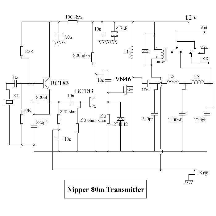
THE NIPPER 3.5Mhz Transmitter

I think that this circuit was developed by G3ROO but my notes are lacking in this information

COMPONENTS LIST

L2,L3 23 turns on a T37-2 Toroid

L1 2 off FX1115 beads side by side with as many turns through as possible

X1 3.5 Mhz Xtal

Relay 12v

Diode across relay 1N4148


http://www.qsl.net/g3pto/nipper.html

Thursday, March 10, 2011

Small FM Transmitter


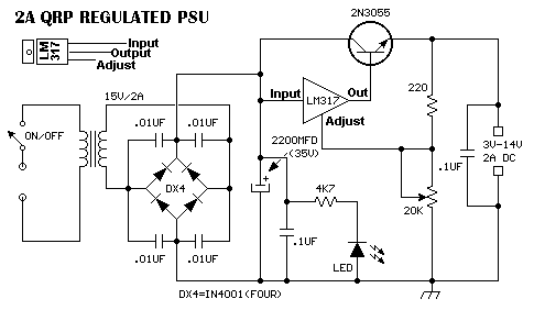
2A Regulated PSU


By Nadisha 4S7NR

Main thing this works, Only thing you will have to find a sutable transformer that gives about 15V(2A) at your house hold power 220V or 110V.

Wednesday, March 9, 2011

Simple RF Detector For 2M


This simple circuit helps you sniff out RF radiation leaking from your transmitter, improper joints, a broken cable or equipment with poor RF shielding. The tester is designed for the 2-m amateur radio band (144-146 MHz in Europe). The instrument has a 4-step LED readout and an audible alarm for high radiation voltages. The RF signal is picked up by an antenna and made to resonate by C1-L1. After rectifying by diode D1, the signal is fed to a two-transistor high-gain Darlington amplifier, T2-T3.
Simple RF Detector For 2M circuit diagram

Assuming that a 10-inch telescopic antenna is used, the RF level scale set up for the LEDs is as follows: When all LEDs light, the (optional) UM66 sound/melody generator chip (IC1) is also actuated and supplies an audible alarm. By changing the values of zener diodes D2, D4, D6 and D8, the step size and span of the instrument may be changed as required. For operation in other ham or PMR bands, simply change the resonant network C1-L1. As an example, a 5-watt handheld transceiver fitted with a half-wave telescopic antenna (G=3.5dBd), will produce an ERP (effective radiated power) of almost 10 watts and an e.m.f. of more than 8 volts close to your head.
Simple RF Detector For 2M

Inductor L1 consists of 2.5 turns of 20SWG (approx. 1mm dia) enameled copper wire. The inside diameter is about 7mm and no core is used. The associated trimmer capacitor C1 is tuned for the highest number of LEDs to light at a relatively low fieldstrength put up by a 2-m transceiver transmitting at 145 MHz. The tester is powered by a 9-V battery and draws about 15mA when all LEDs are on. It should be enclosed in a metal case.

Low Power FM Transmitter


This article should satisfy those who might want to build a low power FM transmitter. It is designed to use an input from another sound source (such as a guitar or microphone), and transmits on the commercial FM band - it is actually quite powerful, so make sure that you don't use it to transmit anything sensitive - it could easily be picked up from several hundred metres away. The FM band is 88 to 108MHz, and although it is getting fairly crowded nearly everywhere, you should still be able to find a blank spot on the dial.
NOTE: A few people have had trouble with this circuit. The biggest problem is not knowing if it is even oscillating, since the frequency is outside the range of most simple oscilloscopes. See Project 74 for a simple RF probe that will (or should) tell you that you have a useful signal at the antenna. If so, then you know it oscillates, and just have to find out at what frequency. This may require the use of an RF frequency counter if you just cannot locate the FM band.

The circuit of the transmitter is shown in Figure 1, and as you can see it is quite simple. The first stage is the oscillator, and is tuned with the variable capacitor. Select an unused frequency, and carefully adjust C3 until the background noise stops (you have to disable the FM receiver's mute circuit to hear this).

Low Power FM TransmitterFigure 1 - Low Power FM Transmitter

Because the trimmer cap is very sensitive, make the final frequency adjustment on the receiver. When assembling the circuit, make sure the rotor of C3 is connected to the +9V supply. This ensures that there will be minimal frequency disturbance when the screwdriver touches the adjustment shaft. You can use a small piece of non copper-clad circuit board to make a screwdriver - this will not alter the frequency.

The frequency stability is improved considerably by adding a capacitor from the base of Q1 to ground. This ensures that the transistor operates in true common base at RF. A value of 1nF (ceramic) as shown is suitable, and will also limit the HF response to 15 kHz - this is a benefit for a simple circuit like this, and even commercial FM is usually limited to a 15kHz bandwidth.

Capacitors
All capacitors must be ceramic (with the exception of C1, see below), with C2 and C6 preferably being N750 (Negative temperature coefficient, 750 parts per million per degree Celsius). The others should be NPO types, since temperature correction is not needed (nor is it desirable). If you cannot get N750 caps, don't worry too much, the frequency stability of the circuit is not that good anyway (as with all simple transmitters).

How It Works
Q1 is the oscillator, and is a conventional Colpitts design. L1 and C3 (in parallel with C2) tunes the circuit to the desired frequency, and the output (from the emitter of Q1) is fed to the buffer and amplifier Q2. This isolates the antenna from the oscillator giving much better frequency stability, as well as providing considerable extra gain. L2 and C6 form a tuned collector load, and C7 helps to further isolate the circuit from the antenna, as well as preventing any possibility of short circuits should the antenna contact the grounded metal case that would normally be used for the complete transmitter.

The audio signal applied to the base of Q1 causes the frequency to change, as the transistor's collector current is modulated by the audio. This provides the frequency modulation (FM) that can be received on any standard FM band receiver. The audio input must be kept to a maximum of about 100mV, although this will vary somewhat from one unit to the next. Higher levels will cause the deviation (the maximum frequency shift) to exceed the limits in the receiver - usually ±75kHz.

With the value shown for C1, this limits the lower frequency response to about 50Hz (based only on R1, which is somewhat pessimistic) - if you need to go lower than this, then use a 1uF cap instead, which will allow a response down to at least 15Hz. C1 may be polyester or mylar, or a 1uF electrolytic may be used, either bipolar or polarised. If polarised, the positive terminal must connect to the 10k resistor.


Inductors

The inductors are nominally 10 turns (actually 9.5) of 1mm diameter enamelled copper wire. They are close wound on a 3mm diameter former, which is removed after the coils are wound. Carefully scrape away the enamel where the coil ends will go through the board - all the enamel must be removed to ensure good contact. Figure 2 shows a detail drawing of a coil. The coils should be mounted about 2mm above the board.
For those still stuck in the dark ages with imperial measurements (grin), 1mm is about 0.04" (0.0394") or 5/127 inch (chuckle) - you will have to work out what gauge that is, depending on which wire gauge system you use (there are several). You can see the benefits of metric already, can't you? To work out the other measurements, 1" = 25.4mm
NOTE: The inductors are critical, and must be wound exactly as described, or the frequency will be wrong.

Figure 2 - Detail Of L1 And L2

The nominal (and very approximate) inductance for the coils is about 130nH.This is calculated according to the formula ...
L = N² * r² / (228r + 254l)
... where L = inductance in microhenries (uH), N = number of turns, r = average coil radius (2.0mm for the coil as shown), and l = coil length. All dimensions are in millimetres.

Pre-Emphasis
It is normal with FM transmission that "pre-emphasis" is used, and there is a corresponding amount of de-emphasis at the receiver. There are two standards (of course) - most of the world uses a 50us time constant, and the US uses 75us. These time constants represent a frequency of 3183Hz and 2122Hz respectively. This is the 3dB point of a simple filter that boosts the high frequencies on transmission and cuts the same highs again on reception, restoring the frequency response to normal, and reducing noise.

The simple transmitter above does not have this built in, so it can be added to the microphone preamp or line stage buffer circuit. These are both shown in Figure 3, and are of much higher quality than the standard offerings in most other designs.

Low Power FM Transmitter

Figure 3 - Mic And Line Preamps

Rather than a simple single transistor amp, using a TL061 opamp gives much better distortion figures, and a more predictable output impedance to the transmitter. If you want to use a dynamic microphone, leave out R1 (5.6k) since this is only needed to power an electret mic insert. The gain control (for either circuit) can be an internal preset, or a normal pot to allow adjustment to the maximum level without distortion with different signal sources. The 100nF bypass capacitors must be ceramic types, because of the frequency. Note that although a TL072 might work, they are not designed to operate at the low supply voltage used. The TL061 is specifically designed for low power operation.
The mic preamp has a maximum gain of 22, giving a microphone sensitivity of around 5mV. The line preamp has a gain of unity, so maximum input sensitivity is 100mV. Select the appropriate capacitor value for pre-emphasis as shown in Figure 3 depending on where you live. The pre-emphasis is not especially accurate, but will be quite good enough for the sorts of uses that a low power FM transmitter will be put to. Needless to say, this does not include "bugging" of rooms, as this is illegal almost everywhere.
I would advise that the preamp be in its own small sub-enclosure to prevent RF from entering the opamp input. This does not need to be anything fancy, and you could even just wrap some insulation around the preamp then just wrap the entire preamp unit in aluminium foil. Remember to make a good earth connection to the foil, or the shielding will serve no purpose.

source: http://sound.westhost.com/project54.htm

Modem Off Indicator


The modem off indicator is intended especially for serious Internet surfers. It will be seen that the circuit of the indicator cannot be much simpler, or there might be nothing left. In spite of its simplicity, it may prove to be a cost-saving device, since it shows at a glance whether the telephone line is free again after the modem has been used. This obviates high telephone charges in case for some reason the modem continues to operate. The circuit depends on the fact that there is a potential of about 40 V on the telephone line when it is not busy. This voltage drops sharply when a telephone call is being made. If, therefore, the circuit is linked to telephone terminals a and b, the lighting of the green LED shows that the line is not busy in error.
Circuit diagram:Modem Off Indicator Circuit Diagram

Modem Off Indicator Circuit Diagram

The bridge rectifier ensures that the polarity of the line voltage is of no consequence. This has the additional benefit that polarity protection for the LED is not necessary. To make sure that the telephone line is not loaded unnecessarily, the LED is a high efficiency type. This type lights at a current as low as 2 mA, and this is, therefore the current arranged through it by resistor R1.


WARNING.
In spite of the liberal age we live in, it is highly probable that in many countries it is not allowed to connect the indicator across the telephone lines. Seek advice of your local telephone company that owns or operates the telephone network.

Soft Start For Torch - Increases The Life Of Torch Bulbs


The halogen or krypton bulbs in modern torches (USA and Canada: flashlights) have a limited life and are not particularly cheap. A simple modification in the torch lengthens the life appreciably. It is a fact of nature that any incandescent bulb has a finite life. However, the bulbs in modern torches (US and Canada: flashlight) have a less-than-average life. The reason for this is that the halogen or krypton bulbs used are operated at over-voltage to give as bright a light as feasible. The life of these bulbs may be extended simply by connecting a resistor in series with the bulb.


For instance, when the battery voltage is 6V and the bulb is a 500mA type, a series resistor of 1Ω will reduce the voltage across the bulb by about 0.5V. This will certainly lengthen the life of the bulb, but it will also cause a reduction in the available brightness. Also, energy is wasted in the resistor (evinced by heat production). Clearly, this is not a very good solution to the problem. A better one is shunting the bulb with a transistor in series with a resistor.
Soft Start For TorchMOSFET:
Another well-known fact is that incandescent bulbs normally burn out when they are being switched on. This is because the resistance of the cold filament is significantly lower than that during normal operation. This results in a switch-on current that is much higher than the normal operating current. Clearly, much is to be gained by damping the switch-on current. The switch-on current may be limited by a simple circuit that is small enough to allow it to be built into most types of torch. As the diagram shows, such a circuit consists of nothing more than a metal-on-silicon-field-effect-transistor, or MOSFET, and a resistor.
Soft Start For Torch - Increases The Life Of Torch Bulbs

The transistor may be almost any current n-channel type that can handle the requisite power. The popular BUZ11 or BUZ10 is eminently suitable for the present application. The requisite limiting of the start-up current is provided by the internal gate capacitance of the transistor in conjunction with the large gate resistor. If needed, a small capacitor may be added between gate and drain. Once the transistor is conducting hard, the remaining losses are negligible. This is true also when the torch is switched off: the quiescent current flowing through the transistor is much smaller than that caused by the self-discharge of the batteries.

Since it is much simpler to break into the positive supply line of a torch than into the negative line, the addition of the limiting circuit makes it necessary for the batteries to be inserted into the torch the other way around from normal (as indicated by the manufacturer). Also, the on/off switch of a modified torch works the other way around from normal. Fitting the modification in some of the popular Mag-Lite torches is fairly straightforward.

After the rubber cover of the on/off switch has been removed, the entire push-button switch mechanism may be removed by releasing a central hexagonal bolt. The switch terminals may serve as soldering supports for the transistor-resistor series network. If it proves impossible to obtain a 47 MΩ resistor, four or five surfacemount-technology (SMT) resistors of 10 MΩ may be linked in series. Such a link works just as well and is almost as small as a normal 47MΩ resistor.

White LED Lamp


Nowadays you can buy white LEDs, which emit quite a bit of light. They are so bright that you shouldn’t look directly at them. They are still expensive, but that is bound to change. You can make a very good solid-state pocket torch using a few of these white LEDs. The simplest approach is naturally to use a separate series resistor for each LED, which has an operating voltage of around 3.5 V at 20 mA. Depending on the value of the supply voltage, quite a bit of power will be lost in the resistors. The converter shown here generates a voltage that is high enough to allow ten LEDs to be connected in series. In addition, this converter supplies a constant current instead of a constant voltage.

A resistor in series with the LEDs produces a voltage drop that depends on the current through the LEDs. This voltage is compared inside the IC to a 1.25-V reference value, and the current is held constant at 18.4 mA (1.25 V ÷ 68 Ω). The IC used here is one of a series of National Semiconductor ‘simple switchers’. The value of the inductor is not critical; it can vary by plus or minus 50 percent. The black Newport coil, 220 µH at 3.5 A (1422435), is a good choice. Almost any type of Schottky diode can also be used, as long as it can handle at least 1A at 50V. The zener diodes are not actually necessary, but they are added to protect the IC. If the LED chain is opened during experiments, the voltage can rise to a value that the IC will not appreciate.
Resistors:
R1 = 1kΩ2
R2 = 68Ω
Capacitors:
C1 = 100µF 16V radial
C2 = 680nF
C3 = 100µF 63V radial
Inductors:
L1 = 200µH 1A
Semiconductors:
D1 = Schottky diode type PBYR745 or equivalent
D2-D5 = zener diode 10V, 0.4W
D6-D15 = white LED
IC1 = LM2585T-ADJ (National Semiconductor)

CRYSTAL TESTER


Figure shows the circuit of a simple crystal tester. It switches on a light emitting diode (LED) if the crystal is working.

The crystal under test is placed in an oscillator circuit. If it is working, an RF voltage will be present at the collector. This is rectified (converted to DC) and made to drive a transistor switch. Applying current to the base causes current to be drawn through the collector, thus lighting the LED.

If an indication of frequency is required, simply use a general coverage receiver to locate the crystal oscillator's output. Note however that when testing overtone crystals (mostly those above 20 MHz) the output will be on the crystal's fundamental frequency, and not the frequency marked on the crystal's case. Fundamental frequencies are approximately one-third, one-fifth or one-seventh the overtone frequency, depending on the cut of the crystal.

The circuit may be built on a small piece of matrix board and housed in a plastic box. Alternatively, a case made from scrap printed circuit board material may be used. Either a selection of crystal sockets or two leads with crocodile clips will make it easier to test many crystals quickly. The RF choke is ten turns of very thin insulated wire (such as from receiver IF transformers) passed through a cylindrical ferrite bead. Its value does not seem to be particularly critical, and a commercially-available choke could probably be substituted.

The circuit can be tested by connecting a crystal known to work, and checking for any indcation on the LED. A shortwave transistor radio tuned near the crystal's fundamental frequency can be used to verify the oscillator stage's operation. Note however that this circuit may be unreliable for crystals under 3 MHz, and some experimentation with oscillator component values may be required.

The crystal checker also tests ceramic resonators. Other applications include use as a marker generator for homebrew HF receivers (use a 3.58 MHz crystal) and as a test oscillator for aligning equipment.

Figure Two:


FIELD STRENGTH METER


A field strength meter is perhaps the simplest piece of RF test equipment that can be built. Used for checking transmitters, antenna experimentation, and testing RF oscillators, field strength meters provide an indication of the presence of RF energy. They are not frequency sensitive and are useful where indication of a change in level is more important than the actual strength of the signal indicated.

Figure One shows a schematic of an RF field strength meter. Like a crystal set, it requires no power source. However, unlike a crystal set, the meter has no tuned circuit. It responds to signals of any frequency.

The meter works by converting any RF signal present at the antenna to a DC voltage. This voltage drives a meter movement to give an indication of relative RF. The meter includes a control to reduce its sensitivity where required.

Because it uses few parts, a printed circuit board is not necessary; components can simply be soldered to one another. However, a box is desirable for operating convenience. The case and aerial from a discarded toy walkie-talkie was used in the prototype (see photograph), though any small plastic case will suffice. The meter movement need not be large; we are only detecting the presence of RF, and not making precise measurements.

A meter from an old radio or tape recorder should work fine. The diodes can be any germanium type; the actual part number is not important. Germanium diodes can be recognised by their 6mm-long clear glass case with two coloured bands towards the cathode end. None of the component values shown are critical; a 50 percent variation would have little effect on circuit operation.

To test the operation of the meter, a transmitter is required to provide a source of RF. Placing the field strength meter's extended antenna near a handheld VHF rig should produce an indication on the meter, assuming that the sensitivity control has been set to maximum. No indication means that the meter is not working. Common construction errors include connecting the diodes or the meter wrongly and using silicon diodes in place of the germanium diodes specified. In this case, the meter will still work, but with reduced sensitivity. The earth wire is optional; when working with low-powered oscillators, it is useful to clip it to ground (of the circuit under test) to ensure a better indication on the meter.

Those without a transmitter can use an RF signal generator or crystal oscillator (such as that described later) for testing purposes. In this case, place the meter's antenna directly on the output terminal to verify operation. However, only attempt this with transistorised circuitry; component ratings and safety considerations make the meter described here unsuitable for poking around valve equipment.

The field strength meter is a useful instrument in its own right, but it can be made more versatile. Modifications include adding an amplifier (for greater sensitivity), including a tuned circuit (so it only detects signals in a particular band), or converting it into an RF wattmeter and dummy load. Circuits for such instruments are found in the standard handbooks.


Signal Frequency Beat Frequency Oscillator


picture of BFO and receiver

The days when you could listen to amateurs on a simple shortwave AM receiver are with us again, thanks to the development of this one-transistor, frequency-agile signal frequency beat frequency oscillator. When teamed up with a low-cost AM set covering 3.5 and 7 MHz, this device provides effective reception of local eighty and forty metre SSB transmissions.

It is an ideal project for the aspiring amateur, as it allows them to monitor amateur activity. Its usefulness, low cost, and ease of construction would make it a good group project for schools, radio clubs or amateur theory classes.

The device is a miniature transmitter. It provides a steady carrier signal to the receiver to replace that suppressed within the transmitter (refer to any radio theory book for a more detailed explanation). It is the ultimate in simplicity, employing but eight components. The unit costs approximately ten dollars to build from all-new parts, and requires no alignment or connections to the receiver. Anyone with basic soldering skills can construct this project, and have it working first time.

Though receivers covering the short wave bands are no longer in every home, suitable sets can be picked up cheaply at garage sales and swap meets. Tuning the medium wave and one or two short wave bands, their performance is lacking in many respects. Nevertheless, they work better than might be expected when used with this circuit. The reasons for this are given later.

image

This unit is a one transistor 3.5 MHz RF oscillator whose frequency can be varied. As mentioned before, it replaces the carrier in the receiver that was suppressed during the transmitter's SSB generation process.

A 3.58 MHz ceramic resonator sets the oscillator frequency. This two-dollar component is similar to a crystal. Its main advantage is that it can be shifted over a 100 kHz frequency range by connecting a variable capacitor in series with it. While the frequency stability is somewhat inferior to that of a crystal, it is still acceptable for stable SSB reception.

Because the BFO operates directly on the received frequency, many of the limitations of low cost AM receivers (such as frequency drift, coarse frequency readout, hand-capacity and difficulty of tuning) are either eliminated or made less apparent. This is because the tuning in of SSB transmissions is effectively performed by a stable, easy to tune BFO, rather than the unstable free-running coarse-tuning local oscillator within the receiver. The latter would have been the case had a conventional 455kHz fixed-frequency BFO been employed.

The circuit shown (see below) covers the popular 3.525 - 3.625 MHz frequency range. This permits reception of CW and SSB activity, WIA Divisional Broadcasts and Morse practice transmissions. The second harmonic of this range covers the 7.050 to 7.250 MHz segment of forty metres, while the fourth might be useable for twenty metre reception.

Construction

Virtually any construction method may be used to assemble the BFO. However, large stray capacitances must be avoided if the full tuning coverage is to be obtained. Several prototypes were built. Almost any construction technique can be used.

Full frequency coverage will only be obtained if leads are kept short. Those to the ceramic resonator and variable capacitor are particularly critical. Whereas most RF projects are built in metal cases to provide shielding, the BFO's operation depends on there being a lack of shielding between it and the receiver. Thus either a plastic or wooden box is recommended.

Testing/Operation

To verify BFO operation, your AM short wave set is required. Position the receiver near the BFO, and tune it across the 3.5 - 4 or 7 - 8 MHz frequency range. At a certain point on the dial, the receiver will go quiet; all normal background noise will be silenced. Switching off the BFO will restore the normal band noise, while adjusting the BFO's 'Tune' Control will move the 'silence' to a different frequency. If the BFO passes these two checks, you know that it works.

Now switch off the BFO, attach a piece of wire (preferably outdoors) to the receiver's telescopic antenna, and tune in a strong SSB signal for maximum volume. Assuming the received signal is within the BFO's tuning range, it will be possible to resolve the signal by correctly adjusting the BFO. Place the BFO near the receiver, and adjust the BFO's tune control until the receiver quietens. Move the BFO away from the set, and adjust it carefully until the SSB signal is intelligible. Note that this setting is critical; the BFO's frequency must be equal to that of the transmitter's suppressed carrier. While at first this process is somewhat fiddly, it becomes easier with practice. For optimum results, experiment with the physical distance between the BFO and the receiver; weaker signals require less signal from the BFO (ie a greater separation). However, it should be possible to find a compromise position for the BFO where reception from all stations is satisfactory.

A novel device to allow the reception of amateur signals on domestic AM-only short wave receivers has been described. It is cheap, very simple to build, and can be expected to work first time. It fills a definite need amongst potential amateurs, and has the advantage of being expandable to a direct conversion receiver or CW/DSB transmitter or transceiver as interest develops.

One Valve CW transmitter


This transmitter was first constructed in 1987 and provided the author with his first 'real' rig, capable of distances of more than about 100 metres. It performed better than expected, with 250km contacts being commonplace and 2500km being occasionally possible.

It consists of a 6GV8 valve, common in the many valve TVs that were rusting in rubbish tips at the time. Unlike some slightly simpler designs, it is a two stage circuit, the triode section being used for the oscillator and the pentode as the power amplifer. With a high tension of about 200 volts power output of about 3 watts could be obtained on 3.5 MHz.

It will work with the cheap 3.58 MHz crystals, but you won't get many contacts up there – better to invest in a lower frequency crystal – eg 3.530 MHz or so. A VXO is not provided – these do not usually provide much shift with 3.5 MHz crystals. However if you wish to add one, wire an inductor (approx 6.8uH) in series with the crystal and add a variable capacitor from point 'A' to earth.

A circuit for a power supply is not included. The one used for this project is based on a transformer from an old valve radio. Use a bridge rectifier and electrolytic capacitor (rated at 350v or so) for smoothing. However as the current drawn is low, even a single 1000v diode will work as the rectifier in this circuit.

Like nearly all valve circuits, this transmitter uses lethal voltages. It should be fully enclosed so that no high voltage points can be touched by the operator. A metal chassis, such as a cake tin is suitable.

To test, insert a crystal, wire a small light bulb (eg dial light) across the antenna terminals and press the key. Adjusting the Tune and Load controls should cause the light to glow quite brightly. Plate current should be around 30-50mA. For the transmit/receiving switching, either have the receiver connected to a separate antenna or use a switch or relay to switch the antenna over.

circuit of 1 valve transmitter

Noice source


clip_image002

A broadband noise source is useful for testing purposes. This circuit gave a reasonably flat output up to 30 MHz when checked with a general coverage receiver. The output impedance is about 50 ohms. It's basically a zener diode used as a noise source with a broadband RF amplifier. I think the higher power zeners give more noise, which is why I used a 1W device. The zener voltage isn't critical, of course; use whatever you have around 6V. The 4:l transformer is 8 bifilar turns on a SiemensEPCOS B64290P37X33 ferrite toroid. An FT37-43 could be used.

Bent Dipole antenna


clip_image002

The simplest way to shorten a dipole is shown in Fig . If you do not have sufficient length between the supports, simply hang as much of the center of the antenna as possible between the supports and let the ends hang down. The ends can be straight down or may be at an angle as indicated but in either case should be secured so that they do not move in the wind. As long as the center portion between the supports is at least ë/4, the radiation pattern will be very nearly the same as a full-length dipole.

The resonant length of the wire will be somewhat shorter than a full-length dipole and can best be determined by experimentally adjusting the length of ends, which may be conveniently near ground. Keep in mind that there can be very high potentials at the ends of the wires and for safety the ends should be kept out of reach.

FM Super regenerative Receiver using only two transistors

The oscillator coil is made from five turns of 0.8 mm (ideally, silver plated) copper wire on a diameter of 8 mm. Short connections are essential, especially to the tuning capacitor: we soldered a trimmer directly to the ground plane. The second coil in the circuit consists of 20 turns of 0.2 mm enamelled copper wire wound on a 10 kÙ resistor. The rest of the circuit is constructed as shown in Figure.

image

The antenna should not be too long, as otherwise the circuit may cause interference: the superregenerative circuit is also a transmitter! Nevertheless the circuit is very sensitive and operates perfectly satisfactorily using a 10 cm length of wire for an antenna. The headphones should ideally have an impedance of at least 400 Ù. The circuit will work with 32 Ù stereo headphones, but the output will not be as loud. It is important to use a transistor designed for radio frequency use (such as the BF494) as it is difficult to get the circuit to work using an ordinary audio frequency device such as the BC548B.

Tuesday, March 8, 2011

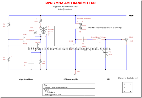
DPN 40M AM Transmitter


image


R1                            1   100R,Resistor (USA Style)
R2                            1   10K,Resistor (USA Style),..
C3                            1   10nf,Capacitor
Q1                            1   2N2222,Bipolar Transistor
L1                            1   30t on 1/2inch PVC pipe,Inductor,..
R3                            1   330R,Resistor (USA Style)
C2                            1   330pF,Capacitor
R4                            1   33K,Resistor (USA Style)
C4                            1   365pF,Capacitor Variable
Q2                            1   BD139,Bipolar Transistor
J1                            1   COAXJ,Coax Jack
G1                            1   GND,Chassis ground
T1                            1   Modulation Transformer,Dual Sec. Transformer w. pins,P
T2                            1   Shortwave,Transformer,4
C1                            1   VC1,Variable Capacitor
X1                            1   XTAL,Crystal

Output power of this transmitter is around 0.8 watts sufficient enough for qrp operation.This circuit uses easily available old radio junks like shortwave osc.coil , audio output transformer, 2J variable gang condensers, which makes your job easy. If you have any suggestions or modification ideas please let me know at bcdxer@hotmail.com.

Thanks

12v TRICKLE CHARGER

12vTrickleCharger
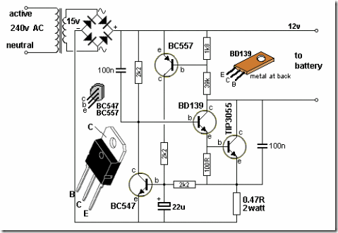
The 12v Trickle Charger circuit uses a TIP3055 power transistor to limit the current to the battery by turning off when the battery voltage reaches approx 14v or if the current rises above 2 amp. The signal to turn off this transistor comes from two other transistors - the BC557 and BC 547.

Firstly, the circuit turns on fully via the BD139 and TIP3055. The BC557 and BC 547 do not come into operation at the moment. The current through the 0.47R creates a voltage across it to charge the 22u and this puts a voltage between the base and emitter of the BC547. The transistors turn on slightly and remove some of the turn-on voltage to the BD139 and this turns off the TIP3055 slightly.

This is how the 2 amp max is created. As the battery voltage rises, the voltage divider made up of the 1k8 and 39k creates a 0.65v between base and emitter of the BC557 and it starts to turn on at approx 14v. This turns on the BC 547 and it robs the BD136 of "turn-on" voltage and the TIP3055 is nearly fully turned off. All battery chargers in Australia must be earthed. The negative of the output is taken to the earth pin.

5-LED CHASER

5-LED-Chaser

The LEDs in this circuit produce a chasing pattern similar the running LEDs display in video shops.

All transistors will try to come on at the same time when the power is applied, but some will be faster due to their internal characteristics and some will get a different turn-on current due to the exact value of the 22u electrolytics. The last 22u will delay the voltage-rise to the base of the first transistor and make the circuit start reliably. The circuit can be extended to any number of odd stages.

MAINS NIGHT LIGHT


LEDNightLight

The circuit illuminates a column of 10 white LEDs. The 10u prevents flicker and the 100R also reduces flicker.

TRANSFORMERLESS POWER SUPPLY


image

This clever design uses 4 diodes in a bridge to produce a fixed voltage power supply capable of supplying 35mA. All diodes (every type of diode) are zener diodes. They all break down at a particular voltage. The fact is, a power diode breaks down at 100v or 400v and its zener characteristic is not useful. But if we put 2 zener diodes in a bridge with two ordinary power diodes, the bridge will break-down at the voltage of the zener. This is what we have done. If we use 18v zeners, the output will be 17v4.

When the incoming voltage is positive at the top, the left zener provides 18v limit (and the left power-diode produces a drop of 0.6v).  This allows the right zener to pass current just like a normal diode but the voltage available to it is just 18v.  The output of the right zener is 17v4. The same with the other half-cycle.

The current is limited by the value of the X2 capacitor and this is 7mA for each 100n when in full-wave (as per this circuit). We have 10 x 100n = 1u capacitance. Theoretically the circuit will supply 70mA but we found it will only deliver 35mA before the output drops. The capacitor should comply with X1 or X2 class. The 10R is a safety-fuse resistor.

The problem with this power supply is the "live" nature of the negative rail. When the power supply is connected as shown, the negative rail is 0.7v above neutral. If the mains is reversed, the negative rail is 340v (peak) above neutral and this will kill you as the current will flow through the diode and be lethal. You need to touch the negative rail (or the positive rail) and any earthed device such as a toaster to get killed. The only solution is the project being powered must be totally enclosed in a box with no outputs.

12v DC to 12v DC BATTERY CHARGER


BatteryCharger
You cannot charge a 12v battery from a 12v battery. The battery being charged creates a "floating charge" or "floating voltage" that is higher than the charging voltage and the charging stops.

The following circuit produces a voltage higher than 12v via a CHARGE PUMP arrangement in which the energy in an electrolytic is fed to a battery to charge it. The circuit produces about 900mA "charge current" and the diodes and transistors must be fitted with heat sinks. The LEDs are designed to prevent the two output transistors turning ON at the same time. The lower output transistor does not start to turn on until the voltage is above 5v and the top transistor does not turn on until the voltage drops 4v from the positive rail. This means both transistors will be turned on when the voltage passes a mid-point-gap of 4v. The transition is so fast that no wasted current (short-circuit current) flows via the two output transistors (as per our test). 

The electrolytic charges to about 10v via the lower transistor and top diode. The top BD679 then pulls the negative of the 2200u electrolytic towards the 12v6 rail and the positive is higher than 12v6 by a theoretical 10v, however we talk about the energy in the electrolytic and in our circuit it is capable of delivering a current flow of about 900mA. This energy is passed to the battery via the lower diode.  Most batteries should not be charged faster than the "14-hour-rate." This basically means a flat battery will be charged in 14 hours. To do this, divide the AHr capacity by 14 to get the charge-rate. For example, a 17AHr battery should be charged at 1.2A or less. For lower-capacity batteries, the 2200u can be reduced to 1,000u. Charging is about 80% efficient. In other words, delivering 120% of the AHr capacity of a battery will fully charge it.  

Thursday, March 3, 2011

FLASHING TWO LEDS

These two circuits will flash two LEDs very bright and consume less than 2mA average current. They require 6v supply. The 330k may need to be 470k to produce flashing on 6v as 330k turns on the first transistor too much and the 10u does not turn the first transistor off a small amount when it becomes fully charged and thus cycling is not produced.
LED_Flasher_2LEDs

IC RADIO

ICradio

This circuit contains an IC but it looks like a 3-leaded transistor and that's why we have included it here.The IC is called a "Radio in a Chip" and it contains 10 transistors to produce a TRF (tuned Radio Frequency) front end for our project.

The 3-transistor amplifier is taken from our SUPER EAR project with the electret microphone removed. The two 1N 4148 diodes produce a constant voltage of 1.3v for the chip as it is designed for a maximum of 1.5v. The "antenna coil" is 60t of 0.25mm wire wound on a 10mm ferrite rod. The tuning capacitor can be any value up to 450p.

1.5v to 10v INVERTER

1v5to9vInverter
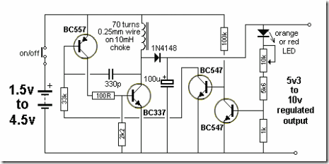
This very clever circuit will convert 1.5v to 10v to take the place of those expensive 9v batteries and also provide a 5v supply for a microcontroller project. But the clever part is the voltage regulating section. It reduces the current to less than 8mA when no current is being drawn from the output. With a 470R load and 10v, the output current is 20mA and the voltage drop is less than 10mV. The pot will adjust the output voltage from 5.3v to 10v.

27MHz TRANSMITTER

27MHzTx
The transmitter is a very simple crystal oscillator. The heart of the circuit is the tuned circuit consisting of the primary of the transformer and a 10p capacitor. The frequency is adjusted by a ferrite slug in the centre of the coil until it is exactly the same as the crystal. The transistor is configured as a common emitter amplifier. It has a 390R on the emitter for biasing purposes and prevents a high current passing through the transistor as the resistance of the transformer is very low. The "pi" network matches the antenna to the output of the circuit.

LED TORCH with ADJUSTABLE BRIGHTNESS

LED-Torch-Cct-AdjBrightness

This circuit will drive up to 3 high-bright white LEDs from a 3v supply. The circuit has a pot to adjust the brightness to provide optimum brightness for the current you wish to draw from the battery. The transformer is wound on a ferrite slug 2.6mm dia and 6mm long as shown in the LED Torch with 1.5v Supply project. This circuit is a "Boost Converter" meaning the supply is less than the voltage of the LEDs. If the supply is greater than the voltage across the LEDs, they will be damaged.

3v WHITE LED FLASHER

3vWhiteLEDflasher
This will flash a white LED, on 3v supply and produce a very bright flash. The circuit produces a voltage higher than 5v if the LED is not in circuit but the LED limits the voltage to its characteristic voltage of 3.2v to 3.6v.   The circuit takes about 2mA an is actually a voltage-doubler (voltage incrementer) arrangement.

Note the 10k in series with the LED charges the 100u. It does not illuminate the LED because the 100u is charging and the voltage across it is always less than 3v. When the two transistors conduct, the collector of the BC557 rises to rail voltage and pulls the 100u HIGH. The negative of the 100u effectively sits just below the positive rail and the positive of the electro is about 2v higher than this. All the energy in the electro is pumped into the LED to produce a very bright flash.

27MHz TRANSMITTER WITHOUT A CRYSTAL

27MHzTx-NoXtal


A 27MHz transmitter without a crystal. When a circuit does not have a crystal, the oscillator is said to be "voltage dependent" or "voltage controlled" and when the supply voltage drops, the frequency changes. If the frequency drifts too much, the receiver will not pick up the signal. For this reason, a simple circuit as shown is not recommended. We have only included it as a concept to show how the 27MHz frequency is generated. It produces a tone and this is detected by a receiver.

LATCHING A PUSH BUTTON


LatchingPushButton

When the circuit is turned on, capacitor C1 charges via the two 470k resistors. When the switch is pressed, the voltage on C1 is passed to Q3 to turn it on. This turns on Q1 and the voltage developed across R7 will keep Q1 turned on when the button is released.
Q2 is also turned on during this time and it discharges the capacitor. When the switch is pressed again, the capacitor is in a discharged state and this zero voltage will be passed to Q3 turn it off. This turns off Q1 and Q2 and the capacitor begins to charge again to repeat the cycle.

TRANSISTOR TESTER

TransistorTester


The 555 operates at 2Hz. Output pin 3 drives the circuit with a positive then zero voltage. The other end of the circuit is connected to a voltage divider with the mid-point at approx 4.5v. This allows the red and green LEDs to alternately flash when no transistor is connected to the tester.

If a good transistor is connected, it will produce a short across the LED pair when the voltage is in one direction and only one LED will flash. If the transistor is open, both LED’s will flash and if the transistor is shorted, neither LED will flash.